The Correct Answer is Option (D)
Currently no explanation available
1. ⇒ (JEE Main 2023 (Online) 6th April Morning Shift)
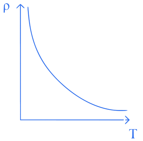
The resistivity of semiconductor varies with temperature. Which of the following curve represents the correct behaviour
A.
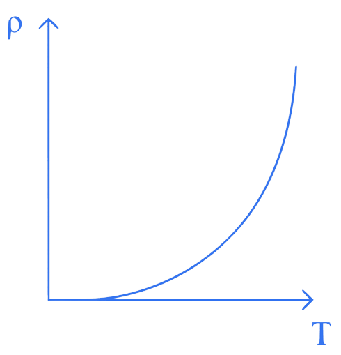
B.
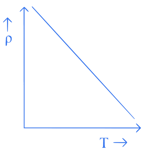
C.
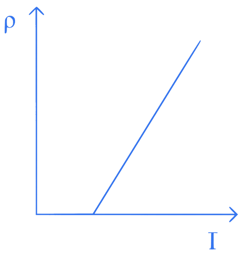
D.
The Correct Answer is Option (D)
Currently no explanation available
2. ⇒ (JEE Main 2023 (Online) 1st February Evening Shift)
Choose the correct statement about Zener diode :
A. It works as a voltage regulator in reverse bias and behaves like simple pn junction diode in forward bias.
B. It works as a voltage regulator in both forward and reverse bias.
C. It works as a voltage regulator only in forward bias.
D. It works as a voltage regulator in forward bias and behaves like simple pn junction diode in reverse bias.
The Correct Answer is Option (A)
Option A is the correct statement about Zener diode. It works as a voltage regulator in reverse bias and behaves like a simple pn junction diode in forward bias. When a Zener diode is reverse-biased, it operates in the breakdown region, where a relatively constant voltage is maintained across the diode, regardless of the current flowing through it. This property makes it useful as a voltage regulator. In forward bias, the voltage applied across the diode is in the same direction as the normal direction of current flow. In this condition, the Zener diode behaves like a simple pn junction diode and allows current to flow in the forward direction.
3. ⇒ (JEE Main 2023 (Online) 31st January Morning Shift)
The effect of increase in temperature on the number of electrons in conduction band () and resistance of a semiconductor will be as:
A. decreases, resistance increases
B. Both and resistance increase
C. increases, resistance decreases
D. Both and resistance decrease
The Correct Answer is Option (C)
As
temperature
increases
increases,
this
results
in
increase
in
conductance.
increases,
increases
and
decreases.
4. ⇒
(JEE
Main
2023
(Online)
25th
January
Evening
Shift)
Statement
I
:
When
a
Si
sample
is
doped
with
Boron,
it
becomes
P
type
and
when
doped
by
Arsenic
it
becomes
N-type
semi
conductor
such
that
P-type
has
excess
holes
and
N-type
has
excess
electrons.
Statement
II
:
When
such
P-type
and
N-type
semi-conductors,
are
fused
to
make
a
junction,
a
current
will
automatically
flow
which
can
be
detected
with
an
externally
connected
ameter.
In the light of above statements, choose the most appropriate answer from the options given below
A. Statement I is incorrect but statement II is correct
B. Both Statement I and statement II are correct
C. Statement I is correct but statement II is incorrect
D. Both Statement I and Statement II are incorrect
The Correct Answer is Option (C)
Statement I is correct but in statement II we cannot detect the current through ammeter thus the statement II is incorrect.
5. ⇒ (JEE Main 2021 (Online) 26th August Morning Shift)
Statement
I
:
By
doping
silicon
semiconductor
with
pentavalent
material,
the
electrons
density
increases.
Statement
II
:
The
n-type
semiconductor
has
net
negative
charge.
In
the
light
of
the
above
statements,
choose
the
most
appropriate
answer
from
the
options
given
below
:
A. Statement - I is true but Statement - II is false.
B. Statement - I is false but Statement - II is true.
C. Both Statement I and Statement II are true.
D. Both Statement I and Statement II are false.
The Correct Answer is Option (A)
Pentavalent
activities
have
excess
free
e
6. ⇒ (JEE Main 2021 (Online) 25th February Evening Shift)
For extrinsic semiconductors; when doping level is increased;
A. Fermi-level of both p-type and n-type semiconductors will go upward for T > TFK and downward for T < TFK, where TF is Fermi temperature.
B. Fermi-level of p-type semiconductor will go upward and Fermi-level of n-type semiconductors will go downward
C. Fermi-level of p and n-type semiconductors will not be affected.
D. Fermi-level of p-type semiconductors will go downward and Fermi-level of n-type semiconductor will go upward.
The Correct Answer is Option (D)
In
n-type
semiconductor
pentavalent
impurity
is
added.
Each
pentavalent
impurity
donates
a
free
electron.
So
the
Fermi-level
of
n-type
semiconductor
will
go
upward.
And
In
p-type
semiconductor
trivalent
impurity
is
added.
Each
trivalent
impurity
creates
a
hole
in
the
valence
band.
So
the
Fermi-level
of
p-type
semiconductor
will
go
downward.
7. ⇒ (JEE Main 2019 (Online) 9th January Morning Slot)
Mobility of electrons in a semiconductor is defined as the ratio of their drift velocity to the applied electric field. If, for an n-type semiconductor, the density of electrons is 1019 m3 and their mobility is 1.6 m2/(V.s) then the resistivity of the semiconductor (since it is an n-type semiconductor contribution of holes is ignored) is close to :
A. m
B. 4m
C. 0.4 m
D. 0.2 m
The Correct Answer is Option (C)
For
semiconductor,
Conductivity,
=
ne
q
e
+
nh
q
h
given
that
semiconductor
is
n-type.
So
contribution
of
holes
is
ignored.
nh
q
h
=
0
=
ne
q
e
Resistivity,
=
=
=
=
=
0.4
m
8. ⇒ (JEE Main 2017 (Online) 8th April Morning Slot)
What
is
the
conductivity
of
a
semiconductor
sale
having
electron
concentration
of
hole
concentration
of
electron
mobility
of
2.0
m2
V1
s-1
and
hole
mobility
of
0.01
m2
V1
s1
?
(Take
charge
of
electronas
1.6
10
19
c)
A. 1.68 (-m)1
B. 1.83 (-m)1
C. 0.59 (-m)1
D. 1.20 (-m)1
The Correct Answer is Option (A)
Conductivity
of
semiconductor,
=
e
=
1.6
1019
(5
1018
2
+
5
1019
0.01)
=
1.6
1.05
=
1.68
9. ⇒ (JEE Main 2016 (Offline))
The temperature dependence of resistance of and undoped in the temperature range is best described by :
A. Linear increases for exponential decrease of
B. Linear decrease for linear decrease for
C. Linear increase for linear increase for
D. Linear increase for exponential increase for
The Correct Answer is Option (A)

10. ⇒ (AIEEE 2007)
Carbon, silicon and germanium have four valence electrons each. At room temperature which one of the following statements is most appropriate ?
A. The number of free electrons for conduction is significant only in and but small in
B. The number of free conduction electrons is significant in but small in and
C. The number of free conduction electrons is negligibly small in all the three.
D. The number of free electrons for conduction is significant in all the three
The Correct Answer is Option (A)
and are semiconductors but is an insulator. Also, the conductivity of and is more than because the valence electrons of and lie in third, fourth and second orbit respectively.
11. ⇒ (AIEEE 2006)
If the ratio of the concentration of electrons to that of holes in a semiconductor is and the ratio of currents is then what is the ratio of their drift velocities?
A.
B.
C.
D.
The Correct Answer is Option (C)