Correct Option is (D)
Currently no explanation available
6. ⇒ (MHT CET 2023 11th May Morning Shift )
In the case of NAND gate, if A and B are the inputs and is the output then
A.
B.
C.
D.
Correct Option is (D)
Currently no explanation available
7. ⇒ (MHT CET 2023 10th May Evening Shift )
The output of an 'OR' gate is connected to both the inputs of a 'NAND' gate. The combination will serve as
A. OR gate
B. NOT gate
C. NOR gate
D. AND gate
Correct Option is (C)
| Output of OR gate | Output of NAND gate |
|---|---|
| 0 | 1 |
| 1 | 0 |
| 1 | 0 |
| 1 | 0 |
Truth table of a NOR gate
| A | B | Y |
|---|---|---|
| 0 | 0 | 1 |
| 0 | 1 | 0 |
| 1 | 0 | 0 |
| 1 | 1 | 0 |
The output matches with that of a NOR gate.
The combination represents a NOR gate.
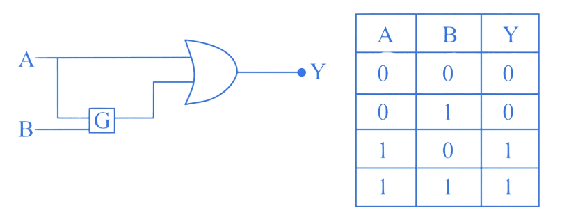
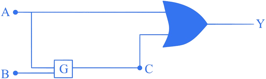
8. ⇒ (MHT CET 2023 10th May Morning Shift )
To obtain the truth-table shown, from the following logic circuit, the gate G should be
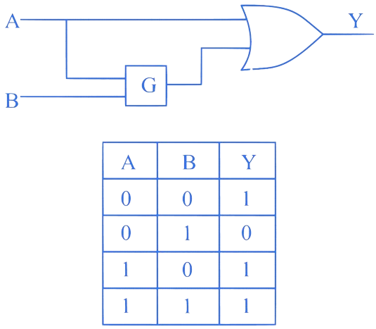
A. AND
B. NAND
C. OR
D. NOR
Correct Option is (D)
The truth table for given configuration is as shown below,
| Case | ||||
|---|---|---|---|---|
| 0 | 0 | |||
| 0 | 1 | |||
| 1 | 0 | |||
| 1 | 1 |
Considering case (I), in order to have output (Y) as has to be 1. For input values, and , if is to be high, the gate could be either NAND or NOR.
Considering case (II), in order to have output (Y) as has to be 0. For input values, and . If is to be 0 , the gate must be NOR.
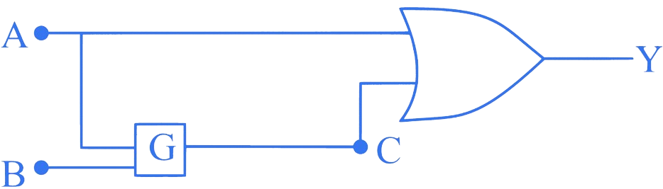
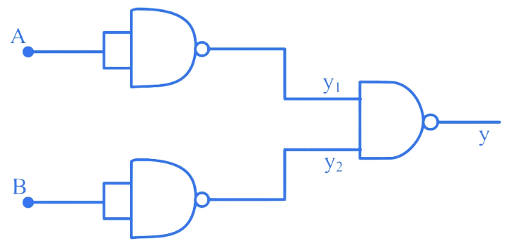
9. ⇒ (MHT CET 2023 9th May Morning Shift )
To get the truth table shown, from the following logic circuit, the Gate G should be
A. OR
B. AND
C. NOR
D. NAND
Correct Option is (B)
Truth table for Y, with the possible values of C is,
| A | C | Y |
|---|---|---|
| 0 | 0 | 0 |
| 0 | 0 | 0 |
| 1 | 0, 1 | 1 |
| 1 | 0, 1 | 1 |
For gate G
| A | B | C | |
|---|---|---|---|
| 0 | 0 | 0 | |
| 0 | 1 | 0 | |
| 1 | 0 | 0, 1 | |
| 1 | 1 | 0, 1 |
is not a NOT gate as NOT gate takes only one input. (II) indicates is not a OR gate as OR gate would give high output for the inputs in (II). Also, (II) indicates it is not a XOR gate as XOR would also give high output for inputs in (II). Hence, the given truth table is satisfied only by AND gate.
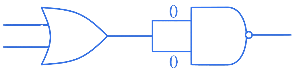
10. ⇒ (MHT CET 2021 21th September Evening Shift )
Combination of NAND gates is shown in the figure. It is equivalent to
A. AND gate
B. NOR gate
C. OR gate
D. X-OR gate
Correct Option is (C)
The two NAND gates whose two inputs are joined together behave like NOT gates. The truth table can be written as
| A | B | y | y | y |
|---|---|---|---|---|
| 0 | 0 | 1 | 1 | 0 |
| 0 | 1 | 1 | 0 | 1 |
| 1 | 0 | 0 | 1 | 1 |
| 1 | 1 | 0 | 0 | 1 |
We see that the output y is '1' if A or B or both are '1'. Hence it behaves as OR gate.