1
. On the basis of electrical conductivity, which one of the following material has the smallest
resistivity?
⇒ (NEET 2023 Manipur)
A. Germanium
B. Silver
C. Glass
D. Silicon
The Correct Answer is Option (B)
Electrical conductivity is a measure of a material's ability to conduct an electric current.
The
higher the
conductivity, the lower the resistivity. So, if we are looking for the material with the
smallest
resistivity, we are looking for the material with the highest electrical conductivity.
Among the options given, silver (Option B) is known to have the highest electrical
conductivity
and thus,
the smallest resistivity. Germanium (Option A) and silicon (Option D) are semiconductors,
meaning they have
moderate conductivity that can be manipulated, while glass (Option C) is generally a poor
conductor, or an
insulator. Therefore, silver is the correct answer.
2 .
A p-type extrinsic semiconductor is obtained when Germanium is doped with: ⇒
(NEET
2023 Manipur)
A. Antimony
B. Phosphorous
C. Arsenic
D. Boron
The Correct Answer is (D)
For p type semiconductor trivalent impurity added
3.
As the temperature increases, the electrical resistance ⇒ (NEET 2022
Phase 1)
A. Increases for both conductors and semiconductors
B. Decreases for both conductors and semiconductors
C. Increases for conductors but decreases for semiconductors
D. Decreases for conductors but increases for semiconductors
The Correct Answer is (C)
As the temperature increases the resistivity of the conductor increases hence the electrical
resistance
increases. However for semiconductor the resistivity decreases with the temperature. Hence
electrical
resistance of semiconductor decreases.
4.
The electron concentration in an n-type semiconductor is the same as hole concentration in a p-type
semiconductor. An external field (electric) is applied across each of them. Compare the currents in
them.
⇒ (NEET 2021)
A. No current will flow in p-type, current will only flow in n-type
B. Current in n-type = current in p-type
C. current in p-type > current in n-type
D. current in n-type > current in p-type
The Correct Answer is (D)
In N type semiconductor majority charge carriers are e and P type semiconductor majority charge
carriers are holes.
I = neAVd = neA (E)
As e >h Ie > Ih
5.
For a p-type semiconductor, which of the following statements is true? ⇒ (NEET
2019)
A. Holes are the majority carriers and trivalent atoms are the dopants.
B. Holes are the majority carriers and pentavalent atoms are the dopants.
C. Electrons are the majority carriers and pentavalent atoms are the dopants
D. Electrons are the majority carriers and trivalent atoms are the dopants.
The Correct Answer is (A)
In p-type semiconductor, an intrinsic semiconductor is doped with trivalent impurities, that
creates
deficiencies of valence electrons called holes which are majority charge carriers.
6.
In a n-type semiconductor, which of the following statement is true. ⇒ (
NEET 2013)
A. Holes are minority carries and pentavalent atoms are dopants.
B. Holes are majority carries and trivalent atoms are dopants.
C. Electrons are majority carries and trivalent atoms are dopants.
D. Electrons are minority carriers and pentavalent atoms are dopants.
The Correct Answer is (A)
In n-type semiconductor, electrons are majority charge carriers and holes are minority charge
carriers and
pentavalent atoms are dopants.
7.
C and Si both have same lattice structure; having 4 bonding electrons in each. However, C is insulator
where
as Si is intrinsic semiconductor. This is because ⇒ (AIPMT 2012
Prelims)
A. In case of C the valence band is not completely filled at absolute zero temperature.
B. In case of C the conduction band is partly filled even at absolute zero temperature.
C. The four bonding electrons in the case of C lie in the second orbit, whereas in the case of Si they
lie in
the third.
D. The four bonding electrons in the case of C lie in the third orbit , whereas for Si they lie in the
fourth
orbit.
The Correct Answer is (C)
Electronic configuration of 6C
6C = 1s2, 2s2 2p2
The electronic configuration of 14Si
14Si = 1s2, 2s2 2p6, 3s2
3p2
As they are away from Nucleus, so effect of
nucleus is low for Si even for Sn and Pb are
almost mettalic.
8.
Pure Si at 500 K has equal number of electron (ne) and hole (nh)
concentrations of 1.5
1016 m3. Doping by indium increases nh to
4.5 1022 m3. The doped semiconductor is of ⇒ (AIPMT 2011
Mains)
A. p-type having electron concentration ne = 5 109 m3
B. n-type with electron concentration ne = 5 1022 m3
C. p-type with electron concentration ne = 2.5 1010 m3
D. n-type with electron concentration ne = 2.5 1023 m3
The Correct Answer is (A)
(ni)2
= ne × nh
(1.5 × 10¹⁶)2
= ne (4.5 × 10²²)
So ne = 5 × 10⁹
Now nh = 4.5 × 10²²
nh ne
Hence, semiconductor is p-type
and ne = 5 × 10⁹ m–3
9.
If a small amount of antimony is added to germanium crystal ⇒ (AIPMT 2011
Prelims)
A. it becomes a p-type semiconductor
B. the antimony becomes an acceptor atom
C. there will be more free electrons than holes in the semiconductor
D. its resistance is increased
The Correct Answer is (C)
If a small amount of antimony is added to
germanium crystal, crystal becomes n-type semiconductor. Hence, there will be more free
electrons
than holes.
10. Which one of the following statement is false ?
A. Pure Si doped with trivalent impurities gives a p-type semiconductor.
B. Majority carries in a n-type semiconductor are holes.
C. Minority carries in a p-type semiconductor are electrons.
D. The resistance of intrinisic semiconductor decreases with increase of temperature. ⇒
(AIPMT 2010 Prelims)
The Correct Answer is (B)
In a n-type semiconductors, electrons are majority carriers and holes are minority carriers.
11. Which one of the following bonds produces a solid that reflects light in the visible region and whose
electrical conductivity decreases with temperature and has high melting point ? ⇒
(AIPMT 2010 Prelims)
A. metallic bonding
B. van der Waal's bonding
C. ionic bonding
D. covalent bonding
The Correct Answer is (A)
In case of metal, conductivity decreases with increase in temperature and metal has high
melting
point.
12. Sodium has body centred packing. Distance between two nearest atoms is 3.7 ⇒ (AIPMT 2009
)
A. 4.3
B. 3.0
C. 8.6
D. 6.8
The Correct Answer is ()
Distance between nearest atoms in body
centred cubic lattice (bcc),
d =
Given d = 3.7
= 4.3
13.
If the lattice parameter for a crystalline structure is 3.6 , then the atomic radius in fcc crystal is ⇒ (AIPMT 2008)
A. 2.92
B. 1.27
C. 1.81
D. 2.10
The Correct Answer is (B)
The atomic radius in a f.c.c. crystal is =
Atomic radius = = 1.27
14.
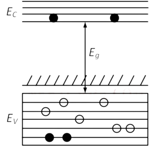
In the energy band diagram of a material shown below, the open circles and filled circles denote holes
and
electrons respectively. The material is ⇒ (AIPMT
2007)
A. an insulator
B. a metal
C. an n-type semiconductor
D. a p-type semiconductor.
The Correct Answer is (D)
For a p-type semiconductor, the acceptor
energy level, as shown in the diagram, is slightly
above the top Ev of the valence band. With very
small supply of energy an electron from the
valence band can jump to the level EC and ionise
acceptor negatively.
15.
For a cubic crystal structure which one of the following relations indicating the cell characteristics
is
correct ? ⇒ (AIPMT 2007)
A. a b c and = = = 90o
B. a = b = c and = 90o
C. a = b = c and = = = 90o
D. a b c and ; = 90o
The Correct Answer is (C)
In a cubic crystal structure
a = b = c and = = = 90o
16 Choose the only false statement from the following. ⇒ (AIPMT 2005)
A. In conductors the valence and conduction bands overlap.
B. Substances with energy gap of the order of 10 eV are insulators.
C. The resistivity of a semiconductor increases with increase in temperature.
D. The conductivity of a semiconductor increases with increase in temperature.
The Correct Answer is Option (C)
Option (a) is correct as in conductor conduction
and valance band overlap and the conduction band
is partially filled
Option (b) is correct as insulators have energy gap
of 5 - 10 eV.
Option (c) is incorrect as resistivity decreases with
increase in temperature.
Option (d) is correct as with increase in temperature,
more and more electrons jump to conduction band,
hence conductivity increases.
17.
Carbon, silicon and germanium atoms have four valence electrons each. Their valence and conduction bands
are
separated by energy band gaps represented by (Eg)C, (Eg)si
and
(Eg)Ge respectively. Which one of the following relationships is true in their
case?
⇒ (AIPMT 2005)
A. (Eg)C > (Eg)Si
B. (Eg)C < (Eg)Si
C. (Eg)C = (Eg)Si
D. (Eg)C < (Eg)Ge.
The Correct Answer is Option (A)
Band gap of carbon is 5.5 eV while that of
silicon is 1.1 eV
(Eg)C (Eg)Si
18.
Copper has face centered cubic (fcc) lattice with interatomic spacing equal to 2.54 . The value of lattice constant for this lattice is ⇒ (AIPMT 2005)
A. 2.54
B. 3.59
C. 1.27
D. 5.08
The Correct Answer is Option (B)
Lattice constant for (f.c.c.)
= a = interatomic spacing = 3.59
19.
In semiconductors at a room temperature ⇒ (AIPMT 2004)
A. the valence band is partially empty and the conduction band is partially filled
B. the valence band is completely filled and the conduction band is partially filled
C. the valence band is completely filled
D. the conduction band is completely empty
The Correct Answer is Option (A)
In semiconductors at room temperature the
electrons get enough energy so that they are able to
over come the forbidden gap. Thus at room
temperature the valence band is partially empty and
conduction band is partially filled. Conduction band
in semiconductor is completely empty only at 0 K.
20.
Number of atom per unit cell in B.C.C. ⇒ (AIPMT 2002)
A. 9
B. 4
C. 2
D. 1
The Correct Answer is Option (C)
In body-centred cubic (b.c.c.) lattice there
are eight atoms at the corners of the cube and one
at the centre.
Therefore number of atom per unit cell
= + 1 = 2
21.
The cations and anions are arranged in alternate form in ⇒ (AIPMT 2000)
A. metallic crystal
B. ionic crystal
C. covalent crystal
D. semi-conductor crystal.
The Correct Answer is Option (B)
In an Ionic crystal, the cations and anions are arranged in alternate form.