The Correct Answer is (D)
In given symbol, emitter current leave from emitter so transistor is NPN
order of doping
order of size
for active mode emitter base junction is forward bias and base-collector junction is reverse bias.
1. ⇒ (NEET 2023 Manipur)
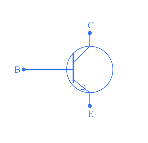
The above
figure
shows the circuit symbol of a transistor. Select the correct statements given below:
(A) The
transistor has two segments of p-type semiconductor separated by a segment of n-type semiconductor.
(B) The emitter is of moderate size and heavily doped.
(C) The central segment is thin
and
lightly doped.
(D) The emitter base junction is reverse biased in common emitter amplifier
circuit.
A. (C) and (D)
B. (A) and (D)
C. (A) and (B)
D. (B) and (C)
The Correct Answer is (D)
In given symbol, emitter current leave from emitter so transistor is NPN
order of doping
order of size
for active mode emitter base junction is forward bias and base-collector junction is reverse bias.
2. For transistor action, which of the following statements is correct?⇒ (NEET 2020 Phase 1)
A. Base, emitter and collector regions should have same size.
B. Both emitter junction as well as the collector junction are forwarded biased.
C. The base region must be very thin and lightly doped.
D. Base, emitter and collector regions should have same doping concentrations.
The Correct Answer is (C)
For transistor action, the input is always forward biased and output is always reverse biased. For this Base has to be very thin and lightly doped.
3. One way in which the operation of a n-p-n transistor differs from that of a p-n-p ⇒ (NEET 2013 (Karnataka))
A. The emitter junction injects minority carries into the base region of the p-n-p
B. The emitter injects holes into the base of the p-n-p and electrons into the base region of n-p-n
C. The emitter injects holes into the base of n-p-n
D. The emitter junction is reversed biased in n-p-n
The Correct Answer is (B)
In p-n-p transistor holes are injected into the base while electrons are injected into the base of n-p-n transistor. Emitter-base junction is forward biased.
4.
Transfer characteristics [output voltage (V0) vs input voltage (Vi)] for a base
biased
transistor in CE configuration is as shown in the figure. For using transistor as a switch, it is used
⇒ (AIPMT 2012 Prelims)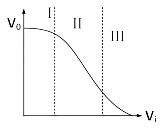
A. in region III
B. both in region (I) and (III)
C. in region II
D. in region I
The Correct Answer is (B)
In the given graph,
Region (I) – Cutoff region
Region (II) – Active region
Region (III) – Saturation region
Using transistor as a switch it is used in cutoff
region or saturation region.
Using transistor as a amplifier it is used in active
region.
5.
For transistor action
(1) Base, emitter and collector regions should have similar size and doping
concentrations.
(2) The base region must be vety thin and lightly doped.
(3) The emitter-base junction is forward biased and base-collector junction is reverse
biased.
(4) Both the emitter-base junction as well as the base-collector junction are forward
biased.
Which one of the following pairs of statements is correct? ⇒ (AIPMT
2010 Mains)
A. (4) and (1)
B. (1) and (2)
C. (2) and (3)
D. (3) and (4)
The Correct Answer is (C)
For transistor action, the base region must be very thin and lightly doped. Also, the emitter-base junction is forward biased and base-collector junction is reverse biased.
6. A n-p-n transistor conducts when ⇒ ( AIPMT 2003)
A. both collector and emitter are positive with respect to the base
B. collector is positive and emitter is negative with respect to the base
C. collector is positive and emitter is at same potential as the base
D. both collector and emitter are negative with respect to the base
The Correct Answer is Option (B)
When the collector is positive and emitter is negative with respect to base, it causes the forward biasing for each junction, which causes conduction of current.