The Correct Answer is Option (D)
AND gate
for AND gate
![]()
1
. The given circuit is equivalent to: ⇒ (
NEET 2023 Manipur)![]()
A.
![]()
B.
![]()
C.
![]()
D.
![]()
The Correct Answer is Option (D)
AND gate
for AND gate
![]()
2.
For the following logic circuit, the truth table is: ⇒ (
NEET 2023)![]()
A.
A
B
Y
0
0
0
0
1
1
1
0
1
1
1
1
B.
| A | B | Y |
|---|---|---|
| 0 | 0 | 1 |
| 0 | 1 | 0 |
| 1 | 0 | 1 |
| 1 | 1 | 0 |
C.
| A | B | Y |
|---|---|---|
| 0 | 0 | 0 |
| 0 | 1 | 0 |
| 1 | 0 | 0 |
| 1 | 1 | 1 |
D.
| A | B | Y |
|---|---|---|
| 0 | 0 | 1 |
| 0 | 1 | 1 |
| 1 | 0 | 1 |
| 1 | 1 | 0 |
The Correct Answer is (A)
Gate
| A | B | Y |
|---|---|---|
| 0 | 0 | 0 |
| 0 | 1 | 1 |
| 1 | 0 | 1 |
| 1 | 1 | 1 |
3. Identify the
equivalent logic gate represented by the given circuit ⇒ (NEET 2022 Phase
2)
![]()
A. NAND
B. OR
C. NOR
D. AND
The Correct Answer is (B)
The given circuit clearly indicates that the bulb will glow when either of the switches are closed.
The corresponding truth table will be
| Input A | Input B | Output Y |
|---|---|---|
| 0 | 0 | 0 |
| 0 | 1 | 1 |
| 1 | 0 | 1 |
| 1 | 1 | 1 |
This suggests that it will correspond to OR gate.
4. The truth table
for the given logic circuit is⇒ (NEET 2022 Phase 1)
![]()
A.
![]()
B.
![]()
C.
![]()
D.
![]()
The Correct Answer is (C)
The truth table would be
![]()
![]()
6.
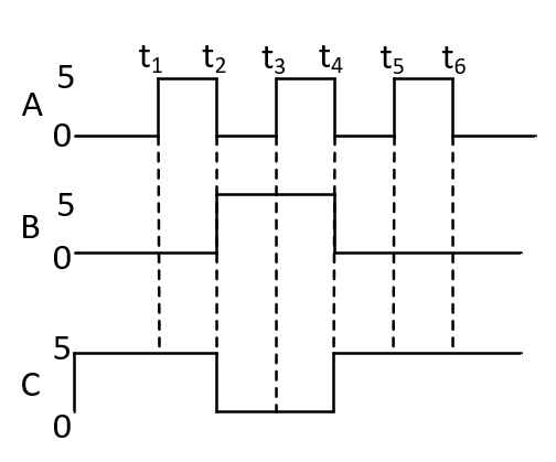
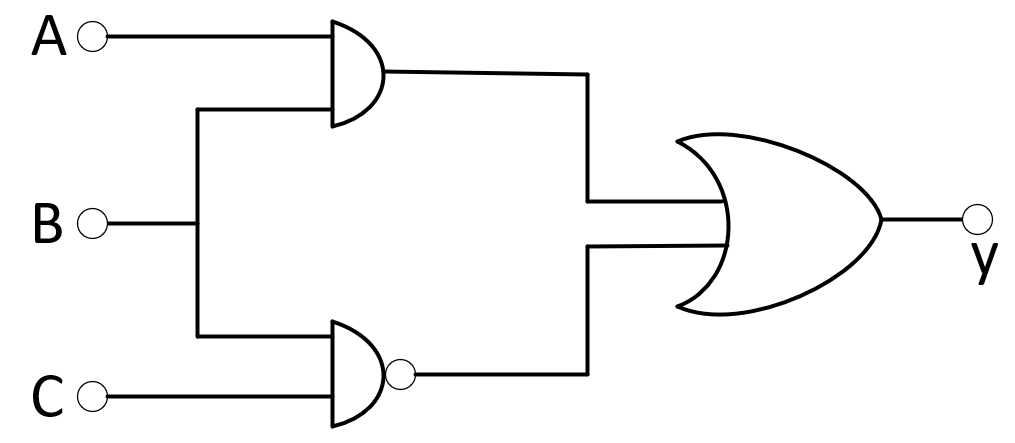
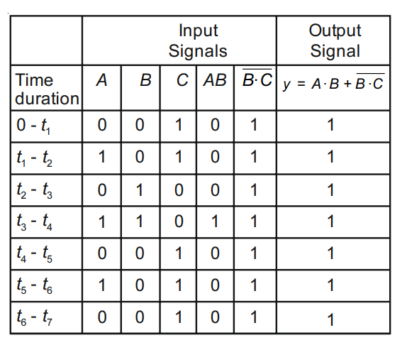
For the given circuit, the input digital signals are applied at the terminals A, B and C. What would be
the
output at the terminal y? ⇒ (NEET 2021)
A.

B.
![]()
C.

D.

The Correct Answer is (C)
7.
The correct Boolean operation represented by the circuit diagram drawn is :⇒
(NEET
2019)
![]()
A. OR
B. NAND
C. NOR
D. AND
The Correct Answer is (B)
From the given logic circuit LED will glow, when voltage across LED in high. This can be verified by the given truth table.
![]()
Boolean expression Y =
This is output of NAND gate.
8.
In the combination of the following gates
the output Y can be written in terms of inputs
A and B as ⇒ (NEET 2018)
![]()
A.
B.
C.
D.
The Correct Answer is ()
![]()
9.
The given electrical network is equivalent to ⇒ (NEET
2017)
![]()
A. OR gate
B. NOR gate
C. NOT gate
D. AND gate
The Correct Answer is (B)
![]()
y1 =
y2 =
=
y = =
So it is NOR gate.
10. For CE transistor amplifier, the aufio signal voltage across the collector resistance of 2 k is 4 V. If the current amplification factor of the transistor is 100 and the base resistance is 1 k, then the input signal voltage is ⇒ (NEET 2016 Phase 2)
A. 10 mV
B. 20 mV
C. 30 mV
D. 15 mV
The Correct Answer is (B)
Voltage gain, A = = = 200
Also, A =
= = 20 mA
11.
What is the output Y in the following circuit, when all the three inputs A, B, C are first 0 and then 1
?
⇒ (NEET 2016 Phase 2)
![]()
A. 0, 1
B. 0, 0
C. 1, 0
D. 1, 1
The Correct Answer is (C)
Applying De Morgan’s law:
Output Y = [(A ⋅ B) ⋅ C]' = A' + B' + C'
When A, B, C are 0 Y = 1
When A, B, C are 1 Y = 0
12.
To get output 1 for the following circuit, the correct choice for the input is
⇒ (
NEET 2016 Phase 1)![]()
A. A = 1, B = 1, C = 0
B. A = 1, B = 0, C = 1
C. A = 0, B = 1, C = 0
D. A = 1, B = 0, C = 0
The Correct Answer is (B)
Output of the circuit, Y = (A + B)·C
Y = 1 if C = 1 and A = 0, B = 1
or A = 1, B = 0 or A = B = 1
13.
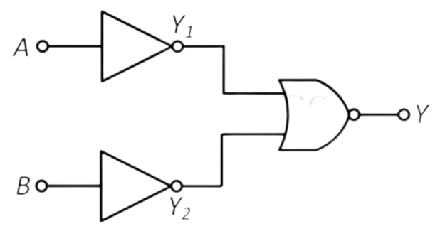
Which logic gate is represented by the following combination of logic gates ?
⇒ (
AIPMT 2015 Cancelled Paper)
A. AND
B. NOR
C. OR
D. NAND
The Correct Answer is (A)
The Boolean expression of this arrangement is
Y = = = A.B
Thus, the combination represents AND gate.
14.
The output from a NAND gate is divided into two in parallel and fed to another NAND gate. The resulting
gate
⇒ (NEET 2013 (Karnataka))
is a
![]()
A. AND gate
B. NOR gate
C. OR gate
D. NOT gate
The Correct Answer is (A)
C' =
C = = A.B
Hence the resultant gate is AND gate.
15.
The output (X) of the logic circuit shown ion figure will be ⇒ (NEET
2013) ![]()
A. X = A . B
B.
C. X =
D. X =
The Correct Answer is (C)
The output of the given logic circuit is
X =
16.
To get an output Y= 1 in given circuit which of the following input will be correct ?⇒
(AIPMT 2012 Mains)
![]()
A. A 1, B 0, C 0
B. A 1, B 0, C 1
C. A 1, B 1, C 0
D. A 0, B 1, C 0
The Correct Answer is (B)
![]()
The
Boolen expression for the given combination is
output Y = (A + B) · C
So it is clear that Y = 1, when A = 1, B = 0 and C = 1
17.
The figure shows a logic circuit with two inputs A and B and the output C. The voltage wave forms across
A,
B
and C are as given. The logic circuit gate is
⇒ (AIPMT 2012 Prelims)
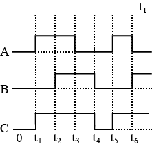
A. OR gate
B. NOR gate
C. AND gate
D. NAND gate
The Correct Answer is (A)
The truth table is
![]()
The logic circuit is OR gate.
18.
Symbolic representation of four logic gates are shown as ⇒ (
AIPMT 2011 Prelims) ![]()
![]()
![]()
![]()
Pick out
which
ones are for AND, NAND and NOT gates, respectively
A. (ii), (iii) and (iv)
B. (iii), (ii) and (i)
C. (iii), (ii) and (iv)
D. (ii), (iv) and (iii)
The Correct Answer is (C)
AND, NAND and NOT gates are (ii), (iv) and (iii) respectively.
19. The following figure shows a logic gate circuit with two inputs A and B and the output Y. The voltage waveforms of A, B and Y are as given.
![]()
The logic
gate
is ⇒ (AIPMT 2010 Mains)
A. NOR gate
B. OR gate
C. AND gate
D. NAND gate
The Correct Answer is (D)
It is clear from given logic circuit, that out put Y is low when both the inputs are high, otherwise it is high. Thus logic circuit is NAND gate.
20. To get an output Y = 1 in given circuit which of the following input will be correct ?
![]() ⇒
(AIPMT 2010 Prelims)
⇒
(AIPMT 2010 Prelims)
A. A 1, B 0, C 0
B. A 1, B 0, C 1
C. A 1, B 1, C 0
D. A 0, B 1, C 0
The Correct Answer is (B)
![]()
The Boolen expression for the given
combination is
output Y = (A + B) · C
So it is clear that Y = 1,
when A = 1, B = 0 and C = 1
21. The device that can act as a complete electronic circuit is ⇒ (AIPMT 2010 Prelims)
A. junction diode
B. integrated circuit
C. junction transistor
D. zener diode
The Correct Answer is (B)
Integrated circuit can act as a complete electronic circuit.
22. The symbolic representation of four logic gates are given below
![]()
The logic symbols
for
OR, NOT and NAND gates are respectively ⇒ (AIPMT 2009)
A. (iv), (i), (iii)
B. (iv), (ii), (i)
C. (i), (iii), (iv)
D. (iii), (iv), (ii)
The Correct Answer is (B)
OR gate, NOT gate and NAND gates are (iv), (ii) and (i) respectively.
23. A transistor is operated in common-emitter configuration at VC = 2V such that a change in the base current from 100 A to 200 A produces a change in the collector current from 5 mA to 10 mA. The current gain is ⇒ (AIPMT 2009)
A. 100
B. 150
C. 50
D. 75
The Correct Answer is (C)
Current gain, =
= = 50
24.
In the following circuit, the output Y for all possible inputs A and B is expressed by the truth table.
⇒ (AIPMT 2007)![]()
A.
B.
C.
D.
The Correct Answer is (C)
Y' =
Y =
Y =
Y = A + B which is OR-gate.
25.
The following figure shows a logic gate circuit with two inputs A and B and the output C. ⇒
(AIPMT 2006)![]()
The voltage
waveforms of A, B and C are as shown below. ![]()
The logic
circuit
gate is
A. OR gate
B. AND gate
C. NAND gate
D. NOR gate
The Correct Answer is (B)
The truth table corresponding to
waveform is given by
The given logic circuit gate is AND gate.
26. The output of OR gate is 1 ⇒ ( AIPMT 2004)
A. if both inputs are zero
B. if either or both inputs are 1
C. only if both inputs are 1
D. if either inputs is zero
The Correct Answer is Option (B)
The truth table of OR gate is
It is seen that output of OR gate is Y = A + B.
If both or any one has 1 input then output will be 1.
27.
The given truth table is for which logic gate
⇒ (AIPMT
2002)
A. NAND
B. XOR
C. NOR
D. OR.
The Correct Answer is Option (A)
This truth table represents NAND gate.
28.
The given truth table is for which logic gate
⇒ (AIPMT
2001)
A. NAND
B. XOR
C. NOR
D. OR
The Correct Answer is Option (A)
This truth table represents NAND gate.
![]()